
Nano-focus Tube of 400 nano resolution is installed which is specialized for Semiconductor Packaging, Wafer Level Packaging (WLP) requiring detection of Sub-micron defects.
Able to trace and inspect defected area precisely by precise movement of axis with Anti-vibration table.
Tomography is available if 3D CT module is added and Wafer Bump Automatic Inspection is available from loading to inspection with wafer handler systems.
Non-destructive analysis system
for Wafer Level Packaging
High resolution image
with Dual Type CTs
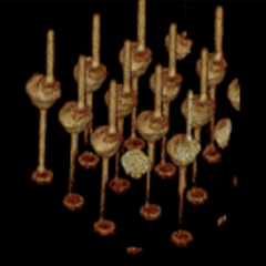
TSV, Micro Bump,
Pattern
TECHNICAL DATA
X-RAY TUBE
120 kV / 200µA
MIN. RESOLUTION
0,2 µm
TABLE SIZE
12 inch (305×305 mm) wafer
DETECTOR
6 inch (152 mm) FPXD
CT SCAN METHOD
Oblique CT
Cone beam CT
AXIS
X, Y, Z Tilt (70º), R
DIMENSIONS
Width: 2380 mm
Length: 1450 mm
Height: 2120 mm
WEIGHT
7000 kg
SAMPLE PHOTOS
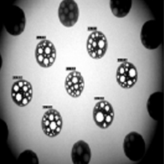
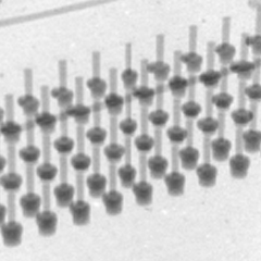
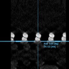
APPLICATIONS
PKG
WAFER
APPLICATIONS
PKG
WAFER